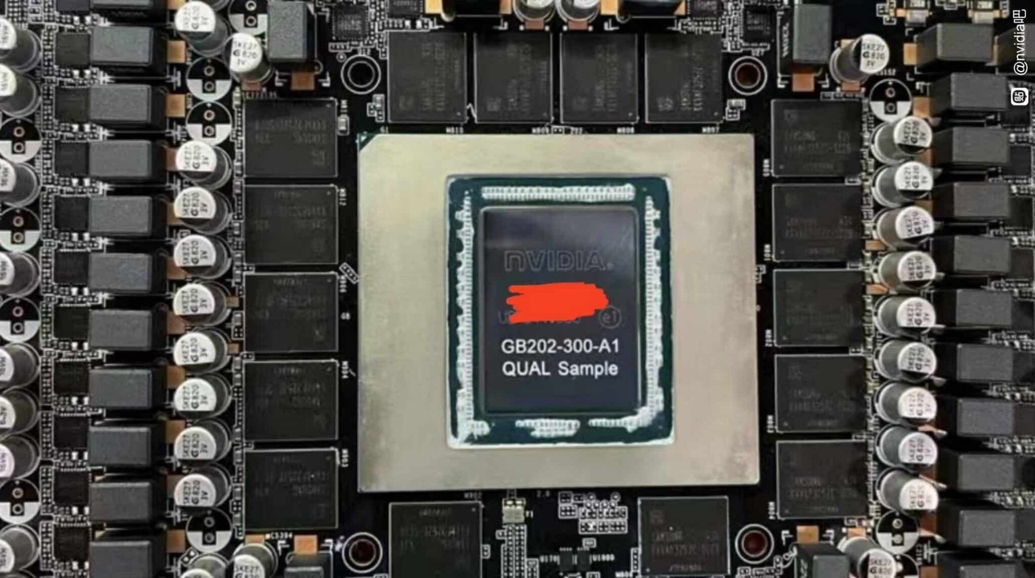
Leaked images of the NVIDIA GeForce RTX 5090 PCB have surfaced online, revealing a massive GB202 “Blackwell” GPU die, Samsung GDDR7 memory chips, and an extensive VRM setup. This leak provides exciting insights into the potential performance and power of NVIDIA’s next-generation flagship graphics card.
The world of PC gaming is abuzz today with the leak of images showcasing the PCB (Printed Circuit Board) of NVIDIA’s upcoming flagship graphics card, the GeForce RTX 5090. This leak, originating from an anonymous source, provides a tantalizing glimpse into the powerhouse that NVIDIA is crafting, potentially set to be unveiled at CES 2025. The images reveal a behemoth of a GPU die, codenamed GB202 “Blackwell,” surrounded by cutting-edge Samsung GDDR7 memory chips and a robust VRM (Voltage Regulator Module) configuration. This leak has ignited a firestorm of speculation and excitement among gamers and tech enthusiasts eager to see what NVIDIA has in store for the future of PC gaming.
What We Know So Far
At the heart of the RTX 5090 lies the GB202-300 silicon, the largest gaming GPU in NVIDIA’s Blackwell lineup. This chip is an absolute monster, boasting an estimated 21,760 CUDA cores, a significant leap from the 18,432 CUDA cores found in the current-generation RTX 4090. The sheer size of the GB202 is awe-inspiring. The physical package measures approximately 63 x 56 mm, while the die itself occupies a substantial 24 x 21 mm area, resulting in a total die size of 744 mm². To put that into perspective, it’s roughly 14% larger than the AD102 die found in the RTX 4090.
Surrounding the massive GPU are 16 Samsung GDDR7 memory chips, confirming the rumored 32 GB memory capacity of the RTX 5090. This is double the amount of VRAM found in the RTX 4090 and will be a boon for gamers playing at high resolutions and demanding workloads like content creation. The memory bus is expected to be 512-bit wide, and with a potential memory speed of 28 Gbps, we could see a staggering memory bandwidth of 1,792 GB/s.
The PCB also reveals a beefy 24-phase VRM solution, hinting at the power demands of this beastly GPU. This draws power from a single 16-pin 12V-2×6 power connector, the new standard for high-end graphics cards.
My Thoughts and Expectations
Having closely followed NVIDIA’s advancements over the years, I’m incredibly excited about the potential of the RTX 5090. The massive increase in CUDA cores, coupled with the GDDR7 memory and robust power delivery, points towards a significant performance uplift over the current generation. I expect to see substantial gains in gaming performance, especially at higher resolutions like 4K and 8K, and even more so in ray tracing and AI-powered workloads.
However, with great power comes great responsibility (and potentially a hefty price tag). The RTX 5090 is likely to be a power-hungry card, and users will need a robust PSU to handle its demands. It’ll be interesting to see how NVIDIA tackles power efficiency and thermals with this new architecture.
A Closer Look at the Details
Let’s delve deeper into the key components revealed in the leaked images:
- GB202 “Blackwell” GPU: This new architecture is rumored to be based on TSMC’s 4N process node, which should offer improved performance and power efficiency compared to the current 5nm process used for Ada Lovelace GPUs. The significant increase in CUDA core count suggests a major architectural overhaul, potentially leading to a substantial performance boost in traditional rasterization, ray tracing, and AI tasks.
- Samsung GDDR7 Memory: GDDR7 memory is the next evolution in graphics memory technology. It promises significantly higher bandwidth and improved power efficiency compared to GDDR6. With a potential data rate of up to 32 Gbps, GDDR7 could unlock new levels of performance in memory-intensive workloads.
- 24-Phase VRM: The extensive VRM setup indicates that NVIDIA is not holding back on power delivery for the RTX 5090. This robust design should ensure stable power delivery even under heavy load, maximizing performance and overclocking potential.
The Future of PC Gaming
The leaked images of the RTX 5090 PCB paint a picture of a graphics card that pushes the boundaries of performance. With its massive GPU die, cutting-edge GDDR7 memory, and powerful VRM setup, the RTX 5090 is poised to be a game-changer for PC gaming.
This leak also raises some intriguing questions. How will NVIDIA price this flagship card? What kind of power consumption and thermals can we expect? And most importantly, how will it perform in real-world gaming scenarios?
We’ll have to wait for NVIDIA’s official announcement to get definitive answers. But one thing is certain: the future of PC gaming looks incredibly exciting.
Beyond the Hardware
While the hardware specifications are undoubtedly impressive, it’s important to remember that the software plays a crucial role in realizing the full potential of any graphics card. NVIDIA has consistently delivered with its software innovations, such as DLSS (Deep Learning Super Sampling) and RTX technologies. I’m eager to see how these technologies evolve with the RTX 5090 and how game developers will leverage the increased horsepower to create even more immersive and visually stunning gaming experiences.
The Impact on the Market
The release of the RTX 5090 is likely to have a significant impact on the graphics card market. It will undoubtedly set a new benchmark for performance, pushing AMD and other competitors to innovate and raise their game. This competition ultimately benefits consumers, as it drives down prices and accelerates technological advancements.
The leaked images of the NVIDIA GeForce RTX 5090 PCB have provided a fascinating glimpse into the future of PC gaming. This card promises to be an absolute beast, pushing the boundaries of performance with its massive GPU die, GDDR7 memory, and robust power delivery. While we await official confirmation from NVIDIA, the excitement and anticipation surrounding the RTX 5090 are palpable. It’s a great time to be a PC gamer!


