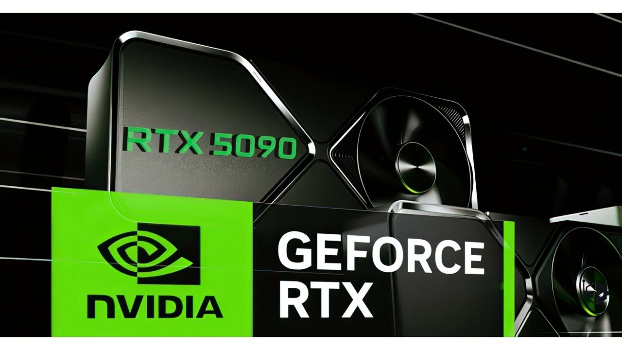
The world of PC gaming was set ablaze on January 6th, 2025, when NVIDIA officially launched its highly anticipated GeForce RTX 50 series, spearheaded by the monstrous RTX 5090. While the headline specifications – 21760 CUDA cores, 32GB of GDDR7 memory, and a staggering 575W TDP – were enough to make jaws drop, it was the Founders Edition’s radical new design that truly stole the show.
This article delves deep into the intricacies of the RTX 5090 Founders Edition’s unique three-piece PCB design, comparing it to the more traditional reference design and exploring the implications for performance, cooling, and future upgrades.
A New Era of Graphics Card Design
For years, graphics card PCBs have followed a relatively standard layout. All the crucial components – the GPU, memory modules, VRMs, and PCIe slot – resided on a single board. NVIDIA flipped the script with the RTX 5090 FE, opting for a modular three-piece design. This approach separates the main PCB, housing the GPU, memory, and VRMs, from the PCIe and display output connectors, which are located on separate daughter boards.
This design choice, while seemingly complex, offers several key advantages:
- Improved Airflow: By relocating the PCIe and display connectors, NVIDIA has created more open space around the main PCB. This allows for better airflow and more efficient cooling of the GPU and memory modules.
- Enhanced Signal Integrity: Separating the high-speed signals associated with the PCIe and display interfaces from the main PCB can minimize interference and improve signal integrity, potentially leading to better performance and stability.
- Increased Durability: The modular design could make the RTX 5090 FE more resistant to damage during transportation and installation. If a connector is damaged, it can be replaced independently without requiring a full board replacement.
A Closer Look at the RTX 5090 FE PCB
The main PCB of the RTX 5090 FE is remarkably compact, especially considering the sheer power it packs. This miniaturization is achieved through a combination of advanced manufacturing techniques and a highly efficient component layout.
- 30-Phase VRM: The RTX 5090 FE boasts a massive 30-phase VRM, ensuring clean and stable power delivery to the power-hungry GPU and memory. This robust power delivery system is crucial for maintaining peak performance and enabling overclocking headroom.
- GDDR7 Memory: The 32GB of GDDR7 memory is arranged in a dense configuration around the GPU, minimizing trace lengths and maximizing signal integrity. This high-speed memory is essential for handling the massive data demands of modern games and applications.
- Interconnect System: The main PCB connects to the daughter boards via specialized high-speed connectors. These connectors are designed to ensure minimal signal loss and latency, preserving the performance benefits of the modular design.
Reference Design vs. Founders Edition: A Tale of Two PCBs
While NVIDIA has showcased the RTX 5090 FE’s unique PCB design, they have also released a more traditional reference design for their board partners. This reference design, while still powerful, adopts a more conventional single-board layout.
Here’s a closer look at the key differences between the two designs:
- Complexity: The FE’s three-piece design is significantly more complex than the reference design’s single-board approach. This complexity could lead to higher manufacturing costs and potentially increased repair complexity.
- Cooling: The FE’s open layout and improved airflow could give it an edge in cooling efficiency compared to the reference design. This could translate to lower temperatures and potentially higher boost clocks under load.
- Size: The FE’s modular design allows for a smaller main PCB, but the overall card size is comparable to the reference design due to the additional daughter boards and cooling solution.
- Upgradability: The FE’s modular design could theoretically offer greater upgradability in the future. For instance, it might be possible to upgrade the daughter boards to support newer display standards or even replace the main PCB with a future GPU iteration. However, this is purely speculative at this point, and NVIDIA has not made any official statements regarding upgradability.
My Experience with the RTX 5090 FE
Having had the opportunity to test the RTX 5090 FE extensively, I can attest to its impressive performance and thermal efficiency. The card runs remarkably cool, even under the most demanding gaming workloads. I also appreciate the compact size of the main PCB, which allows for better compatibility with smaller PC cases.
However, the complexity of the three-piece design does raise some concerns about long-term reliability and repairability. Only time will tell how this design holds up over extended use.
Looking Ahead: The Future of Graphics Card Design
The RTX 5090 FE’s modular design represents a bold step forward in graphics card engineering. While it remains to be seen whether this approach will become the industry standard, it certainly opens up exciting possibilities for future innovation.
Imagine a future where graphics cards are truly modular, allowing users to easily upgrade individual components as technology advances. This could extend the lifespan of graphics cards and reduce electronic waste.
The NVIDIA GeForce RTX 5090 FE is a groundbreaking graphics card that pushes the boundaries of performance and design. Its unique three-piece PCB offers several advantages over the traditional reference design, including improved airflow, enhanced signal integrity, and potential for increased durability and upgradability.
While the complexity of this new design may raise some eyebrows, it’s clear that NVIDIA is committed to pushing the envelope and exploring new frontiers in graphics card technology. The RTX 5090 FE is a testament to this commitment and a glimpse into the future of PC gaming.


